
TB-303: tracing the oscillator, filter and amplifier
Following the original service schematic from pitch conversion through the loaded filter, envelopes and output stage.
Technical research · edition 2 · reviewed 2026-10-24
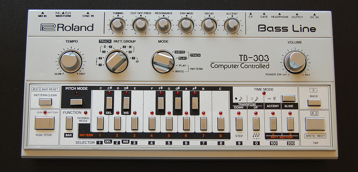
Steve Sims, TB303 Front View (2008), dedicated to the public domain. Image source. View full-size image

What we found
Our TB-303 reconstruction showed why the familiar “oscillator into four low-pass stages” description is insufficient. The ladder stages load one another, the cutoff control supplies current rather than a directly specified frequency, and the envelope and amplifier draw current from shared nodes. Those interactions have to survive any reduction intended for realtime use.
We traced the service drawing, compared independent BA662 reconstructions, and built a connected nominal reference with 118 unknown voltages and 36 passive capacitor currents. The most concrete correction was a transistor-half wiring discrepancy in a published BA662 transcription. The sections below give the useful equations, that correction, and the electrical evidence. They describe a nominal engineering model, not component measurements from an original unit.
Deriving the loaded ladder
This is a conditional ladder core, not yet the complete TB-303 VCF. It lives in
PL-33/source/circuit/ladder.h. The signal path surrounding Q12-Q23, Q19-Q21,
feedback coupling capacitors, cutoff current generator and finite base currents
must still be composed before treating it as the production filter.
Assume matched ideal exponential junctions, infinite beta, no Early effect or junction capacitances, a prescribed total ladder current I, and a fixed top common bias. These are explicit nominal semiconductor assumptions. Differential voltage v[k] is the left-minus-right voltage of each physical rung capacitor, bottom first. The physical capacitors are 18, 33, 33, 33 nF. Both arms and the current drawn by the next rung are retained. Thermal voltage is nominally 25.85 mV.
For arm currents L and R with L+R=I, the ideal diode equation gives deltaV=VTlog(L/R), hence L-R=Itanh(deltaV/(2*VT)). Define:
The factor two comes from subtracting the two arm KCL equations: each capacitor current appears with opposite signs. The returned voltage uses a positive core orientation; any following differential-amplifier inversion is external.
Trapezoidal integration solves all four states simultaneously. Endpoint current history retains the old input and old tail current across automation edges. Newton is limited to 12 iterations and 0.1 V maximum node increments. Acceptance requires a maximum differential-current residual below 1e-13 A; rejection retains all capacitor voltages and previous currents. This component's retained-state failure is not yet a complete product recovery policy.
Independent checks must use a linear nodal admittance solve or a continuous-time ODE, not the same Newton implementation. For a steady input at nonzero I, all four fluxes equal Jin; each adjacent voltage drop equals input, giving v=[4,3,2,1]*input. This DC identity is a useful nonlinear check.
Stinchcombe's published C/2 simplification is useful for an independent limiting case; production uses the schematic's 18 nF instead of silently replacing it with 16.5 nF. His analysis also establishes why independent unloaded one-pole stages cannot represent this topology. See the source ledger in README.md.
Evidence: research/tb303/LADDER.md.
A BA662 wiring error and its correction
tools/read_ba662_reference.py reads the archive as data, resolves all 46 XME
connector compositions, and compares terminal connectivity with the PCB. It does
not execute or unpack the project. The comparison finds one wiring discrepancy:
MetaMorph joins Q7.E1/Q9.C1 to Q8.B2, while the PCB joins them to Q8.B1.
Both sources put Q8.C1 at pin 5 and Q8.E1 at pin 8. Consequently the XME connects
the base of the wrong transistor half and leaves the buffer's active base open.
The published Eagle schematic export repeats that discrepancy.
Use the PCB connection: Q8.1 forms the single PNP output transistor; Q8.2 is
unused. There are 17 active transistors, not 18 independently connected ones.
All other core terminal groups agree after excluding R3/R4. The generated
local-references/ba662-connectivity.json retains both the original transcription
and the PCB comparison so the correction remains reviewable.
Pin names are BA662 package pins. N09–N16 and N20 retain the comparison report's internal names; N17–N19 were isolated terminals from the erroneous/unused half. These Q identifiers belong to the clone assembly, not the TB-303 PCB Q numbers.
| Transistor | Polarity | Collector | Base | Emitter |
|---|---|---|---|---|
| Q1.1 | NPN | N09 | Pin1 | Pin5 |
| Q1.2 | NPN | Pin1 | Pin1 | Pin5 |
| Q2.1 | NPN | N10 | Pin2 | N09 |
| Q2.2 | NPN | N11 | Pin3 | N09 |
| Q3.1 | PNP | N10 | N12 | Pin9 |
| Q3.2 | PNP | N12 | N12 | Pin9 |
| Q4.1 | PNP | N11 | N13 | Pin9 |
| Q4.2 | PNP | N13 | N13 | Pin9 |
| Q5.1 | PNP | N14 | N10 | N12 |
| Q5.2 | PNP | Pin6 | N11 | N13 |
| Q6.1 | NPN | N14 | N15 | Pin5 |
| Q6.2 | NPN | N15 | N15 | Pin5 |
| Q7.1 | NPN | Pin9 | Pin7 | N16 |
| Q7.2 | NPN | Pin6 | N14 | N15 |
| Q8.1 | PNP | Pin5 | N16 | Pin8 |
| Q9.1 | NPN | N16 | N20 | Pin5 |
| Q9.2 | NPN | N20 | N20 | Pin5 |
R1 is 47 kohm from Pin4 to N20; R2 is 10 kohm from Pin9 to Pin8. The TB-303 externally joins OTA output Pin6 to buffer input Pin7. Keep them separate in the component model, and join them in the actual surrounding circuit. Its Pin1 mirror accepts the volume/accent current; this should replace the ideal control-pin voltage, including both mirror base currents and actual collector load.
Evidence: research/tb303/BA662-REFERENCE.md.
Connecting the circuit without losing its state
The Q36 volume output, Q38 collector, VR7 accent wiper and both VCF taps become shared nodes. Current from both sides contributes to each shared KCL equation. BA662 pins 6 and 7 are one node, with both original rows and columns summed. Package supplies connect to the fixed supply rails. Digital gate remains an ideal 0/6-V control source, distinct from Q37's collector. Mix In remains the external audio source. The previous optional volume/accent current loads must be zero in this specialization, preventing duplicate external loading.
The added output controls are volume electrical fraction, external Mix In,
line termination and the declared IC14 small-signal input termination.
Refer to VCA-OUTPUT.md (VCA-OUTPUT.md, retained research) for components, capacitor orientations,
the R125 correction and the incomplete LA4140 boundary. VR8's mechanical
A-taper mapping is still separate from its implemented electrical fraction.
Conditional stage startup solutions provide voltage guesses. A final joint 154-variable modified nodal solve holds all 36 capacitor voltages and the oscillator's initial phase while solving the remaining algebraic voltages and all capacitor branch currents. No settling time is skipped. Supplies are already established; this is a powered-on initialization, not a supply ramp. Startup workspaces allocate off the audio thread. Processing uses fixed storage.
Each accepted interval solves the complete circuit with trapezoidal passive capacitor currents and the existing oscillator charge law. Gate prediction includes the VCA clamp and Q38/D36 trigger cathode; predictions change only the Newton starting point. A failed search retains the same physical equations and capacitor history during bounded source continuation and interval subdivision. The existing 2-pA current and 20-nV Newton correction limits are unchanged. Invalid controls retain the last physical state; reset restores all initial voltages, currents and gate prediction history.
The adaptive reference solver remains too expensive to claim production realtime readiness. Finite iteration/subdivision bounds do not establish an acceptable worst-case audio callback duration. Internal-rate convergence, reconstruction, broad automation and CPU measurements remain open gates.
Evidence: research/tb303/COMPLETE-VOICE.md.
What the independent audit established
The 2026-09-13 Release audit passes over 9,292 accepted intervals and 58 independent local roots. Maximum physical KCL error is 1.9948583e-12 A; capacitor-current disagreement is zero at recorded precision; maximum charge error is 2.1175824e-22 C and compensated-update error is 3.4978416e-15 V. Startup algebraic KCL is 8.5032364e-15 A. Independent roots differ by at most 4.3724242e-9 V, with maximum reference KCL 1.9834738e-12 A. The smallest accepted interval is 9.9341075e-12 s, reinforcing the unresolved production CPU boundary.
PL33CompleteVoiceBench renders 4,096 frames at 48 kHz in 64-frame groups,
including the gate, accent and control schedule used above. Preparation is
excluded; parameter updates and all circuit processing are included. Run the
Release executable after other circuit audits finish. This is a workstation
measurement, not a DAW callback test or a universal worst-case guarantee.
On the Ryzen 7 5800X workstation, one 2026-09-13 run took 3.08232 s for
0.0853333 s of audio: 36.1209 times realtime. The slowest group took 0.358976 s
against a 0.00133333-s deadline. Maximum per-frame solve count was 1,297.
The benchmark executable SHA-256 is
873493f0e530d909511ce25b654487ceb76f01d46b2133e5372cf2fbd2b9f4cf;
the raw output is build/tb303-circuit-vs2022/evidence/complete-voice/cpu.txt.
This implementation is therefore a validated reference, not the production
audio callback engine. Reduction/solver scheduling must be checked against
these electrical traces and independent equations before a realtime claim.
Evidence: research/tb303/COMPLETE-VOICE.md.
Applying the findings
For another analog model, start with physical capacitor voltages and node currents. When two subcircuits meet, sum their KCL contributions at the shared node; do not connect two ideal voltage outputs and assume loading is preserved. Keep package pins separate until the surrounding schematic joins them. A useful implementation check is the ladder's nonlinear DC identity above, followed by an independent linear admittance or continuous-time solve.
The BA662 comparison also provides a practical reverse-engineering method: reconcile terminal connectivity across schematic, machine-readable netlist and PCB before fitting transistor parameters. A small wiring error can otherwise be “corrected” by an implausible device fit.
Limits and open questions
The oscillator, cutoff control and output network retain declared semiconductor and load assumptions. The isolated ladder omits finite transistor beta; the assembled reference goes beyond that component boundary. The reference's excellent discrete residuals do not establish continuous-time convergence, measured hardware fidelity, or acceptable callback cost. The separate numerical-methods article examines those distinctions; PL-33's reduced playback engine has its own scope.
Research illustrations
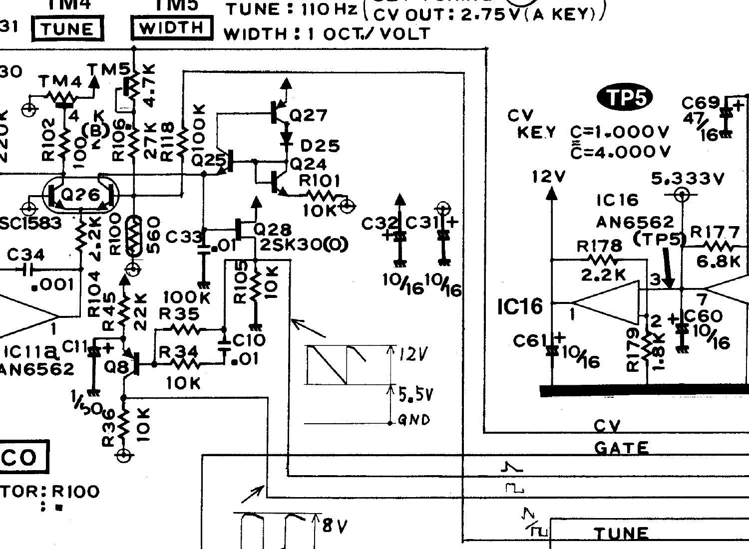
Roland TB-303 service notes: oscillator detail inspected during the circuit investigation. Image source. View full-size image
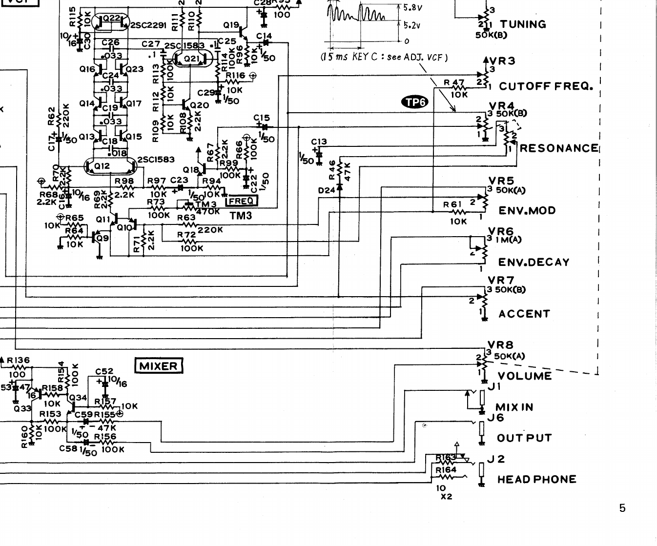
Roland TB-303 service notes: ladder/filter detail used in the nominal reconstruction. Image source. View full-size image
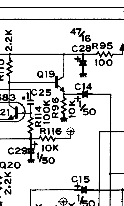
Roland TB-303 service notes: resistor values compared with the independent BOM and circuit analysis. Image source. View full-size image
Primary references
- Roland TB-303 service notes
- Tim Stinchcombe: diode-ladder analysis
- RE-303 official BOM, original TB-303 column
Research provenance
The methods and results above are drawn from these retained research records. Dates and product versions inside the article identify the scope of each experiment; publication review does not mean the hardware or numerical tests were rerun.
research/tb303/LADDER.md— SHA-2566e5adc414372618baf7f76da9548020e7234a9a4f6f6d145f559d35d8bcbfac3research/tb303/BA662-REFERENCE.md— SHA-256219559b1bbe7bf65c300b431d3dc35d0b1c455adf3d217fb609bd7cf1cc050edresearch/tb303/COMPLETE-VOICE.md— SHA-256c70009562d676305501cb6b4c87e2b57ede228651986854e6f843f3ac3c1c3a2