
TR-808 clap: comparator timing and the C140 discrepancy
Tracing the clap envelope while retaining a conflict between the schematic value and service-description timing.
Technical research · edition 2 · reviewed 2026-10-24
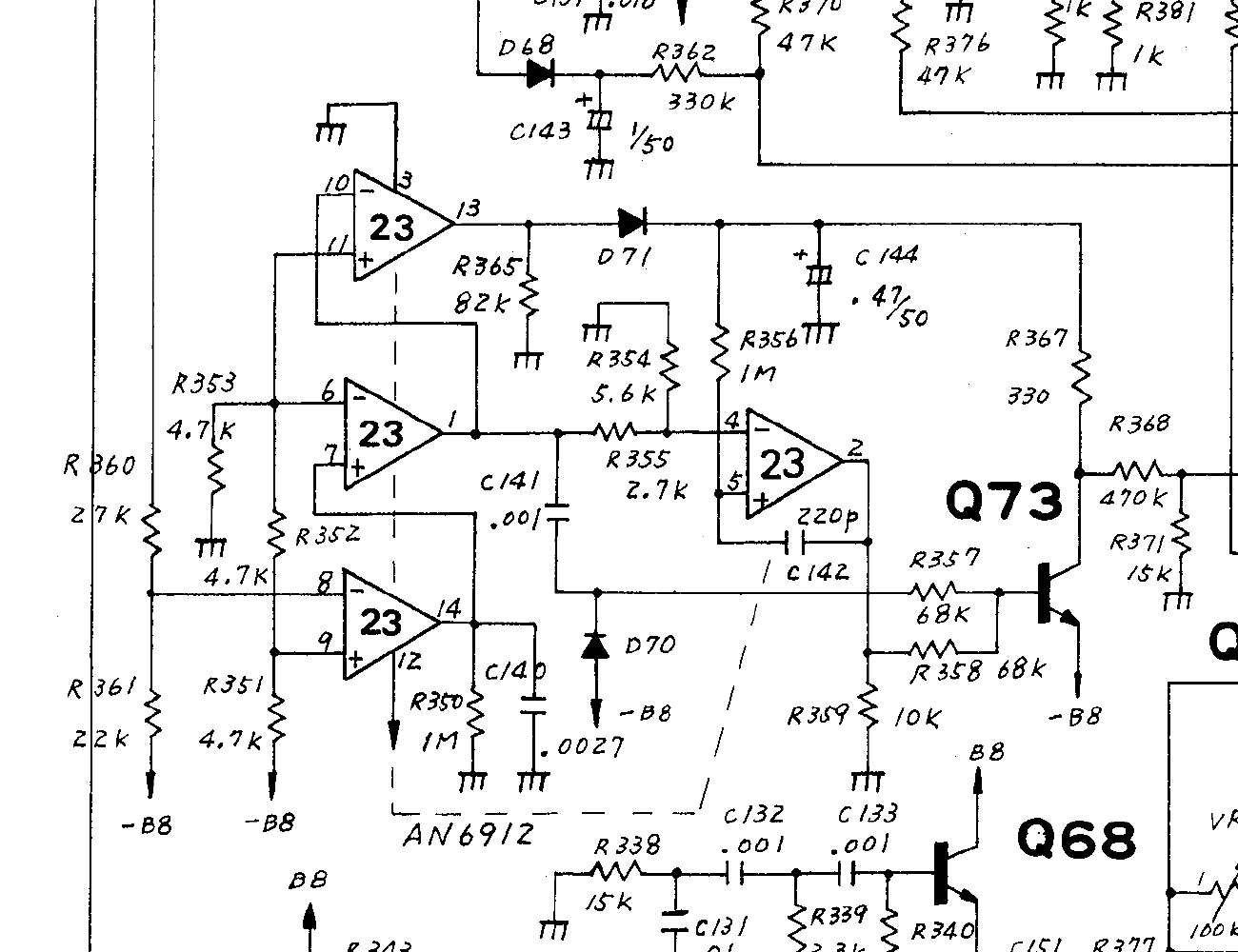
Roland TR-808 service notes: comparator and timing network inspected in the clap-envelope investigation. Image source. View full-size image
What we found
The clap research uncovered a conflict in the original service notes and a consequential schematic crossing. The drawing's 2.7 nF timer gives about 3 ms recovery, while the functional explanation describes roughly 30 ms. Separately, R356 crosses a wire without connecting to it: C142 is its own feedback state, not extra capacitance in parallel with the main envelope capacitor.
Those findings change the model. Repeated bursts arise from threshold crossings and coupled capacitor/transistor behavior, while the reverberant noise branch starts from the same trigger. Scheduling three synthetic bursts followed by a reverb tail misses both relationships.
The circuit nodes and component values
All voltages below are relative to ground. Use V− = −15 V, V+ = +15 V;
IC23 itself has pin 3 at ground and pin 12 at −B8. Define these named nodes so
that the capacitor states and wire crossings remain unambiguous:
| Symbol | Electrical node |
|---|---|
T | CP trigger after SW12, also Q69 base |
v8 | IC23 pin 8, R360/R361 junction |
r | IC23 output 14, input 7, C140 top |
w | IC23 output 1, input 10, C141 top |
t | IC23 input 4, R354/R355 junction |
u | IC23 output 13, D71 anode |
e | C144 top, D71 cathode, R356/R367 ends |
f | IC23 input 5, R356/C142 junction |
z | IC23 output 2, C142/R358/R359 junction |
d | C141 bottom, D70 cathode, R357 end |
b, c | Q73 base and collector; emitter is at V− |
a | C143 top and D68 cathode |
b1, b2, E | Q71 base, Q72 base, their shared emitters |
h, n | C139 top and C138 top, respectively |
b70, x | Q70 base and noise-divider end of C137 |
R356 crosses the wire to pin 4 without a junction. R356 connects e to
the separate pin-5 node f; C142 connects f to output z. Consequently,
C142 is a distinct feedback capacitor, not capacitance in parallel with C144.
Q72 senses Q73's collector c through R368, not C144's node e directly;
R367 separates the two. These details are visible in the p.9 schematic.
Roland schematic, p.9
| Network | Printed components and endpoints |
|---|---|
| Reference ladder | Ground → R353 4.7 kΩ → pin 6/11 → R352 4.7 kΩ → pin 9 → R351 4.7 kΩ → V− |
| Trigger comparator | R360 27 kΩ from T to v8; R361 22 kΩ from v8 to V−; R350 1 MΩ and C140 .0027 µF from r to ground |
| Moving threshold | R355 2.7 kΩ from w to t; R354 5.6 kΩ from t to ground |
| Envelope return | R365 82 kΩ from u to ground; D71 anode u, cathode e; C144 .47 µF from e to ground |
| Fast feedback | R356 1 MΩ from e to f; C142 220 pF from f to z |
| Reset transistor | R367 330 Ω from e to Q73 collector c; Q73 emitter at V− |
| Reset base drive | C141 .001 µF from w to d; D70 anode V−, cathode d; R357 68 kΩ from d to b; R358 68 kΩ from z to b; R359 10 kΩ from z to ground |
| Current converter | R368 470 kΩ from c to b2; R371 15 kΩ from b2 to ground; R366 15 kΩ from V+ to E; Q71 collector at V−; Q72 collector supplies OTA control current |
| Offset and accent | TM3 10 kΩ between ground and V−, wiper through R370 47 kΩ to b1; R364 2.2 kΩ from b1 to ground; R362 330 kΩ from a to b1; C143 1 µF from a to ground |
| Common envelope source | Q69 collector at V+, base T; emitter drives both D68 anode and D69 anode; D68 cathode is a, D69 cathode is h |
| Reverb shaping | C139 .018 µF from h to ground; R348 1 MΩ h → n; C138 .047 µF from n to ground; R349 1 MΩ n → b70 |
| Reverb audio input | C137 .033 µF from x to b70; R342 15 kΩ from filtered noise to x; R346 680 Ω from x to ground, earlier value 1 kΩ |
This ledger follows printed p.9 and its revision annotations. The p.15 design changes independently identify the R346 change. Q70 has a 10 kΩ collector load R363 to V+ and a 330 Ω emitter resistor R369 to ground; the annotated later circuit adds a separate 10 kΩ emitter load to V−. Its collector couples through C152 4.7 nF and R376 47 kΩ to the common summing node, alongside the OTA branch through C150 1 nF and R378 100 kΩ. C146 and the remaining downstream loads must also be retained when implementing that complete audio branch. Roland schematic and changes, pp.9, 15
Evidence: research/drums/808-CLAP-ENVELOPE-NOTES.md.
Timer thresholds expose the source conflict
Neglecting input bias currents in the reference network gives
θ6 = θ11 = −5 V and θ9 = −10 V. The moving threshold is
t = w R354/(R354 + R355). An ideal w = −15 V therefore gives
t = −10.1204819277 V; it is not exactly −10 V. Finite output saturation
changes w and must change t with it.
An ideal comparator sinks when its non-inverting input is lower than its inverting input. The four sections consequently have these sink conditions:
| Output | Non-inverting input | Inverting input | Ideal sink condition |
|---|---|---|---|
Pin 14, r | Pin 9, θ9 | Pin 8, v8 | θ9 < v8 |
Pin 1, w | Pin 7, r | Pin 6, θ6 | r < θ6 |
Pin 13, u | Pin 11, θ6 | Pin 10, w | θ6 < w |
Pin 2, z | Pin 5, f | Pin 4, t | f < t |
Use consistent crossing/equality handling in a hybrid solver; these equations
do not establish an additional arbitrary hysteresis band. Real offset, delay
and input currents require declared device laws. Open collector means release
when off, not an actively driven 0 V output. As a simple illustration, if Q73
has a conducting base at −14.3 V, R359 and R358 alone put released z at
−14.3 × 10/(10 + 68) = −1.833333 V, before the other transient loads.
The trigger divider gives
Thus a positive pulse imposed on a hard 0 V idle would keep pin 14 sinking
between hits. The schematic uses Q29's switched collector, which releases
when off, and the divider returns the un-driven CP node negative. Q69 and its
two diode branches load the actual trigger. Use a declared current/impedance
boundary for Q29 or an explicitly measured CP-node waveform. The source's
1 ms common-trigger duration does not establish arbitrary voltage-source
amplitude or impedance at T.
Roland trigger circuitry and timing, pp.9, 14
After release of pin 14, the ideal isolated timer is
For r0 = −15 V, the logarithm is ln(3). The literal 2.7 nF gives
2.966253179 ms after release; the inferred 27 nF gives 29.662531794 ms. A
1 ms trigger adds 1 ms to each onset-to-window-end duration. Finite pin-14
saturation, incomplete recharge during a retrigger, and loading alter r0;
do not reset a synthetic 30 ms counter on every hit.
Evidence: research/drums/808-CLAP-ENVELOPE-NOTES.md.
The capacitor equations behind repeated bursts
The following are derived KCL equations for the transcribed network, with
ideal references but otherwise unspecified finite semiconductor laws. They
are a model contract, not a claim that the ideal laws below reproduce the
hardware. A prime denotes a time derivative. S14, S1, S13, S2 are
positive open-collector sink currents from their nodes toward V−, controlled
by the comparator conditions. D71(u−e) flows u → e; D70(V−−d) flows
V− → d. I5 is input-5 current leaving f, including any chosen input
junction model. Other input currents are neglected only for these equations.
IB73 and IC73 leave those nodes into the NPN device; saturation, reverse
operation and junction charge need a declared model. In a quasi-static
forward-active approximation IC73 = β IB73, limited by collector compliance.
That approximation alone does not establish turn-off or storage time.
During the low w window, pin 13 releases. R365 and D71 can then return a
negative e toward ground. If f rises through t, pin 2 releases and the
R358 base drive turns on Q73, pulling c and then C144 negative. C142 carries
output transitions into the distinct f state, so neither the Q73 pulse width
nor the next threshold crossing is determined by R365 C144 alone. The
R356 C142 product is 220 µs, a separate fast scale.
When w rises at the timer crossing, pin 13 sinks and D71 becomes reverse
biased for the ordinary negative-envelope range, removing the R365 return
path. C141 carries the positive w edge into d, supplying another Q73 base
transient. Its duration follows the stored capacitor voltage and transistor
load; it is not a separately scheduled final burst. D70 constrains the
opposite d excursion. With ideal instantaneous output transitions, capacitor
continuity gives Δf = Δz and Δd = Δw; finite output slew and junction
currents replace those instantaneous jumps in a complete model.
This exposes a significant limitation of an ideal comparator model. The
conditional simulation below drives f to approximately +13.1 V on a rising
edge and toward −23.3 V on a falling edge before its optional lower clamp.
IC23 runs from 0 V to −15 V: the positive excursion is outside its specified
common-mode range, and the negative excursion is below its stated absolute
input limit. A hypothetical lower clamp at −15.3 V is useful only as a
sensitivity test. It neither specifies an actual diode nor resolves the
positive-input behavior. A production reconstruction must state and test a
finite input/output model in these regions.
Panasonic input limits and comparator data
Evidence: research/drums/808-CLAP-ENVELOPE-NOTES.md.
The current converter loads the envelope
Let TM3's electrical fraction toward V− be p. Its unloaded Thevenin values
are Voff = p V− and Rt = p(1−p) × 10 kΩ. The following includes the pot's
source resistance, the accent capacitor and finite PNP base currents. Positive
IB71 and IB72 are currents injected by the PNPs into their base nodes:
For matched, forward-active, quasi-static PNP devices only, a conditional law
is ICi = Is exp((E−bi)/VT), IBi = ICi/β, and
IEi = (1 + 1/β) ICi. It gives
IC72/IC71 = exp((b1−b2)/VT), but the resistor equations and emitter-current
sum must still be solved. The Q72 collector current controls the BA662 OTA;
it is not a simple linear copy of C144 voltage. Early effect, mismatch,
temperature, collector compliance and storage remain transistor-model choices.
The complete BA662/audio stage is a separate model boundary.
The static diagnostic solves this loaded pair using logarithmic current-domain
Newton iteration and independently using nested voltage-domain bisection.
With Q73 off, the path from e to b2 includes R367 + R368. It uses
explicit assumptions Is = 10⁻¹⁴ A, VT = 25.85 mV, midpoint TM3, and the
chosen β; these are not measured Roland transistor values.
| C144 voltage | β | Conditional Q72 current, accent a = 0 V |
|---|---|---|
| −14.8 V | Infinite | 0.982557 mA |
| −14.8 V | 200 | 0.924180 mA |
| −10 V | Infinite | 0.413609 mA |
| −10 V | 200 | 0.290703 mA |
| 0 V | Infinite | 4.5947 nA |
| 0 V | 200 | 6.7714 nA |
Across β = 50, 100, 200, 500 and infinite, five envelope voltages, and three
additional accent voltages, the two numerical solves differ by at most
5.414 × 10⁻¹⁵ A. This verifies the conditional algebra independently; it
does not validate the chosen transistor parameters. At e = −14.8 V, β200,
the converter path supplies about 30.64 µA into the negative envelope node.
Its base-current loading affects both gain conversion and the capacitor
trajectory and must be coupled back into the full transient solve.
Evidence: research/drums/808-CLAP-ENVELOPE-NOTES.md.
Reverb begins in parallel
Q69's emitter feeds D68 and D69 concurrently. D68 charges the accent branch C143; D69 charges reverb capacitor C139. The reverb path consequently starts from the same trigger event as the repeated-envelope system, not from a timer after the last burst. C139/R348/C138/R349 and the Q70 load shape its evolution. Roland clap explanation and schematic, pp.6, 9
Writing v69 for Q69's emitter and vnoise for the filtered-noise source:
For the later annotated Q70 emitter network,
e70/R369 + (e70−V−)/Radded − IE70 = 0, with Radded = 10 kΩ;
omit that additional branch for the earlier revision. Collector KCL includes
R363 and the C152/C146/downstream current, not an unloaded collector voltage.
Q69 must supply the sum of the D68/D69 currents; a finite source model must
also include Q69 base current in the CP-node loading.
As an isolated passive check only, ground b70, switch off D69 after an
instantaneous h = 10 V, and start n = 0 V. The two-capacitor matrix is
Its poles are −84.0443501551 and −14.0643968898 s⁻¹. Separate RK4 integration
at 5 µs and an eigenvalue matrix exponential agree within 10⁻¹⁰ V over the
checked 0–100 ms points. n is already 0.202622 V after 1 ms and 1.749516 V
after 30 ms: this verifies simultaneous launch of the reduced branch. Actual
Q69 charge, Q70 base current and the noise coupling change these values.
Evidence: research/drums/808-CLAP-ENVELOPE-NOTES.md.
Applying the findings
The isolated timer gives a quick reproducible check: t = R*C*ln(3) for recovery from −15 V to −5 V. With 1 MΩ and 2.7 nF, this is 2.966 ms; substituting 27 nF gives 29.663 ms. The latter explains the functional description but remains an inference, not a verified component correction.
In a hybrid circuit simulator, identify capacitor states and comparator events separately. Open-collector outputs release rather than drive a high voltage. Retain the load seen by each envelope node, check common-mode excursions, and compare threshold times under retrigger. For a simplified sound-design model, use these findings to choose simultaneous branches and stateful burst timing, while labeling the simplification.
Limits and open questions
The equations use node names from the retained schematic ledger: r is the timer/C140 node; w is the window output; e is C144; f is the separate C142 feedback input; z is its comparator output; c is Q73's collector. The published component discrepancy remains unresolved. Ideal comparator excursions leave the datasheet's valid input region, so a calibrated finite device law is still needed. The conditional Q72 currents and passive reverb checks verify algebra, not recorded clap fidelity.
Research illustrations
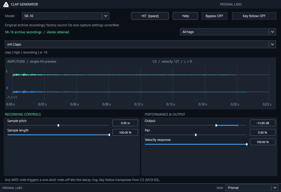
Prismal Labs native editor capture, illustrating the corresponding software project. View full-size image
Primary references
Research provenance
The methods and results above are drawn from these retained research records. Dates and product versions inside the article identify the scope of each experiment; publication review does not mean the hardware or numerical tests were rerun.
research/drums/808-CLAP-ENVELOPE-NOTES.md— SHA-256d1773a8fb588642375bd9c997657b89af70c8cf77e5043513f25d59b182d91c6